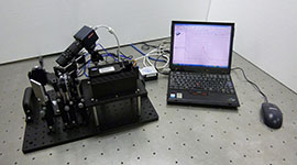
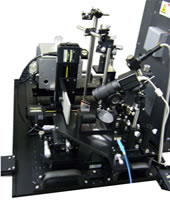
UV-Excited Photoluminescence Measurement System |
||||||||
Model: MUVPL-375 |
||||||||
|
||||||||
■Specifications |
||||||||
|
||||||||
*Specifications and appearance are subject to change without notice for improvement. |
||||||||
Model: MUVPL-193 |
||||||||
|
||||||||
■Specifications |
||||||||
|
||||||||
*Specifications and appearance are subject to change without notice for improvement. |
||||||||
Model: MUVPL-213/325 |
||||||||
|
||||||||
■Specifications |
||||||||
|
||||||||
*Specifications and appearance are subject to change without notice for improvement. |
||||||||
■Basic Principle of Photoluminescence (PL) |
||||||||
|
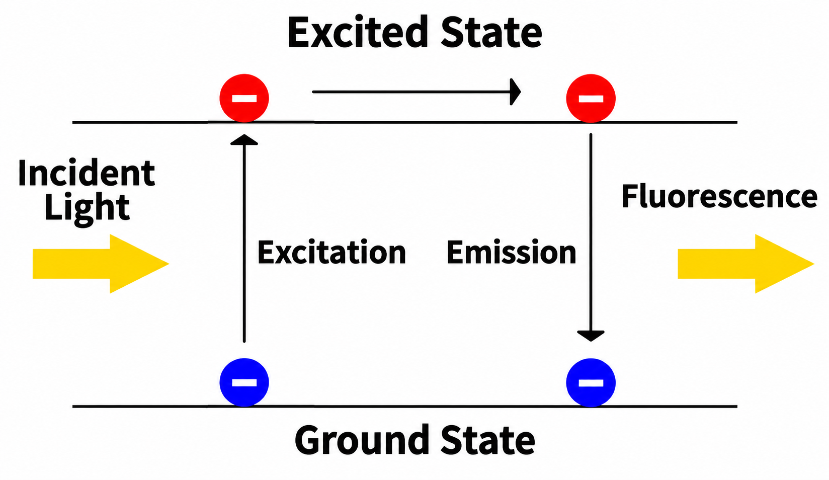
Photoluminescence (PL) is an optical technique in which a material is irradiated with high-energy light (excitation light), exciting electrons in the valence band to higher energy levels such as the conduction band, and the light (photons) emitted as they return to the ground level is detected and analyzed. This phenomenon is widely used to evaluate electronic states and diagnose material quality, mainly in semiconductor materials and phosphors. As shown in the figure, electrons at the ground level (in most cases, the top of the valence band) absorb the energy of the externally applied excitation light and are excited to a higher energy level (typically the conduction band). This creates electron-hole pairs.
However, excited electrons do not necessarily recombine immediately and undergo radiative transitions. In many cases, they pass through relaxation mechanisms such as those shown below before recombining.
Because of these processes, the emission spectrum observed in PL measurements does not necessarily directly reflect the energy difference between the incident photons and the band gap, but is influenced by the various relaxation pathways within the material. PL is a highly sensitive evaluation technique that can be applied to samples without contact or damage. In addition to analyzing band structures and energy levels, it can comprehensively provide information on crystallinity, defect density, impurity distribution, and more. It is regarded as an especially important technique for materials development and quality control of semiconductor devices, and for the evaluation of quantum dots and low-dimensional structures. |
||||||||