
Microscopic Time-Resolved Free Carrier Absorption Measurement System |
||||||||||||||||||||||||||||||||
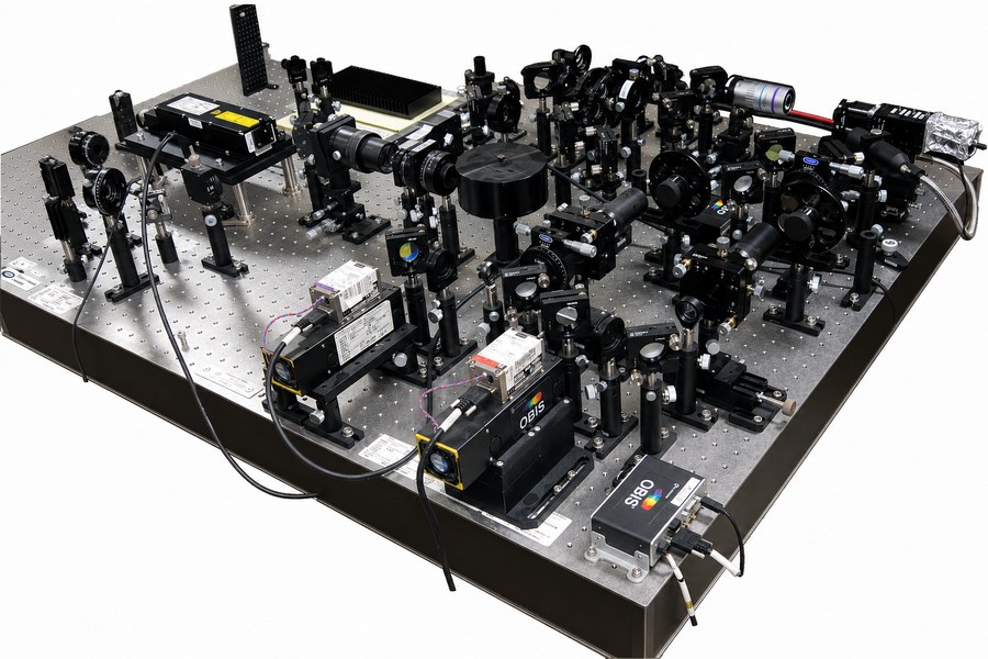 |
||||||||||||||||||||||||||||||||
| This microscopic time-resolved measurement system uses pulsed laser excitation and time-resolved free carrier absorption (TR-FCA) to evaluate carrier recombination processes in semiconductor materials with high spatial resolution. A 355 nm pulsed YAG laser (pulse width: 1 ns, repetition rate: 100 Hz) is used as the excitation source to generate excess carriers in the sample. A 405 nm continuous-wave (CW) laser is used as the probe light, and the time-dependent change in transmitted light intensity due to free carrier absorption is measured with a high-speed photodetector. By analyzing the time-dependent change in probe-light transmittance after excitation, carrier lifetimes can be evaluated without contact or damage to the sample. The spot size of the excitation light can be changed with a variable aperture, and the light is focused precisely onto the sample by the microscope optics. The probe light is focused to approximately 1 μm and overlapped with the excited region, enabling measurement of carrier lifetime distributions with high spatial resolution. By scanning the sample on the stage, carrier lifetime distributions can be evaluated in both the depth and in-plane directions. This microscopic time-resolved free carrier absorption measurement system is well suited to carrier lifetime evaluation, carrier lifetime distribution measurement, defect evaluation, and crystal quality evaluation of wide-bandgap semiconductor materials, including SiC. |
||||||||||||||||||||||||||||||||
■Features |
||||||||||||||||||||||||||||||||
|
• Time-resolved optical excitation with a 355 nm pulsed YAG laser • Time-resolved free carrier absorption (TR-FCA) measurement with a 405 nm CW laser • High-spatial-resolution measurement with microscope optics • Non-contact, non-destructive evaluation using the time-dependent change in free carrier absorption • Measurement of carrier lifetimes and carrier lifetime distributions • Optimization of the measurement area with a variable excitation spot size • Ideal for evaluating wide-bandgap semiconductor materials such as SiC |
||||||||||||||||||||||||||||||||
■Specifications |
||||||||||||||||||||||||||||||||
|
||||||||||||||||||||||||||||||||
*Specifications and appearance are subject to change without notice for product improvement. |
