
Deep-Level Measurement System for Nitride Semiconductors |
||||||||||||||||||||||||||||||||||||||||||||||||||||||||||||||||||||||||||||||||
 |
||||||||||||||||||||||||||||||||||||||||||||||||||||||||||||||||||||||||||||||||
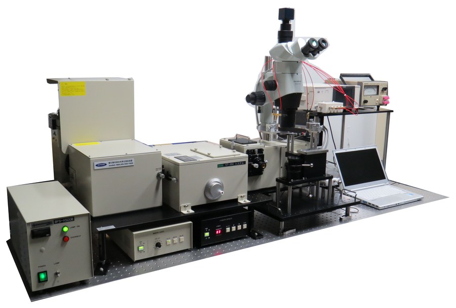
| Deep-level optical spectroscopy (DLOS) is a spectroscopic technique for evaluating deep-level defects in semiconductors by optical excitation. By irradiating the sample with monochromatic light while continuously varying the photon energy and measuring changes in the depletion-layer capacitance, the energy levels and densities of deep-level defects within the band gap can be evaluated. In DLOS measurements, when electrons (or holes) trapped at deep-level defects in the depletion layer absorb the photon energy of the incident monochromatic light and are excited to the conduction band (or valence band), the space-charge distribution in the depletion layer changes. As a result, the depletion-layer width changes, which is detected as a change in junction capacitance. By analyzing the photon-energy dependence of this capacitance change, the optical ionization energies and densities of deep-level defects can be evaluated with high sensitivity. This system consists of a manual probe station for optical characterization and a monochromatic light irradiation unit, and can perform DLOS measurements on semiconductor devices fabricated at the wafer level. By measuring capacitance with high precision while irradiating the sample with monochromatic light, deep-level defects in semiconductors can be analyzed non-destructively. The system is well suited to evaluating crystal defects, impurity levels, and process-induced defects in a variety of semiconductor materials and devices, such as Si, SiC, and GaN, and is an effective analytical system for semiconductor materials research and development, device development, and quality and reliability evaluation. |
||||||||||||||||||||||||||||||||||||||||||||||||||||||||||||||||||||||||||||||||
■Features |
||||||||||||||||||||||||||||||||||||||||||||||||||||||||||||||||||||||||||||||||
|
• Enables evaluation of deep-level defects by deep-level optical spectroscopy (DLOS). • Measures capacitance with high precision while sweeping the photon energy of monochromatic light. • Evaluates the optical ionization energies and densities of deep-level defects. • Supports non-destructive measurement of semiconductor devices fabricated at the wafer level. • Suitable for defect analysis of various semiconductor materials and devices, such as Si, SiC, and GaN. |
||||||||||||||||||||||||||||||||||||||||||||||||||||||||||||||||||||||||||||||||
■Specifications |
||||||||||||||||||||||||||||||||||||||||||||||||||||||||||||||||||||||||||||||||
|
||||||||||||||||||||||||||||||||||||||||||||||||||||||||||||||||||||||||||||||||
*Specifications and appearance are subject to change without notice for product improvement. |
